


Tunnel diode, also known as Esaki diodes (named after the Japanese physicist Leo Esaki who discovered them in 1958), are unique semiconductor devices that exhibit negative resistance in their voltage-current characteristics. This property makes them incredibly useful in high-frequency applications, microwave oscillators, and fast-switching circuits.
In this article, we will explore the construction, working principle, characteristics, advantages, disadvantages, and applications of tunnel diodes in detail.
1. What is a Tunnel Diode?
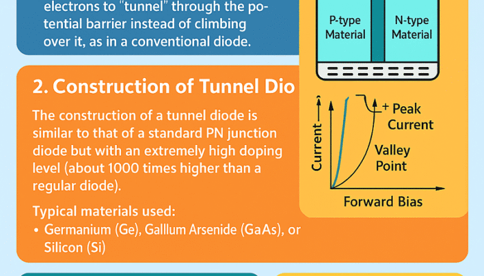
A tunnel-diode is a type of PN junction diode that is heavily doped with impurities. This heavy doping results in a very narrow depletion region, allowing electrons to “tunnel” through the potential barrier instead of climbing over it, as in a conventional diode.
This tunneling phenomenon is a direct result of quantum mechanics and gives the diode its distinctive negative resistance behavior.
2. Construction of Tunnel Diode
The construction of a tunnel diode is similar to that of a standard PN junction diode but with an extremely high doping level (about 1000 times higher than a regular diode).
- P-type Material: Doped with acceptor impurities.
- N-type Material: Doped with donor impurities.
- Depletion Region: Extremely narrow due to heavy doping.
The typical materials used are Germanium (Ge), Gallium Arsenide (GaAs), or Silicon (Si).
3. Working Principle of Tunnel-Diode
The operation of a tunnel diode relies on quantum tunneling. When a small voltage is applied:
- Zero Bias Condition
At zero voltage, some electrons from the conduction band of the N-region align with the empty states in the valence band of the P-region, allowing tunneling to occur. - Forward Bias (Initial Region)
As voltage increases slightly, tunneling becomes significant, causing current to rise rapidly. - Peak Current Point
At a certain voltage, the tunneling current reaches a maximum (called peak current). - Negative Resistance Region
Beyond the peak, increasing voltage actually causes the current to drop. This is the negative resistance region, which is the key to oscillation and amplification applications. - Valley Point
After this region, normal diode conduction resumes as electrons gain enough energy to overcome the potential barrier.
4. V-I Characteristics of Tunnel Diode
The voltage-current curve of a tunnel diode has three main regions:
- Forward Bias Positive Resistance Region (small voltage, increasing current).
- Negative Resistance Region (current decreases as voltage increases).
- Forward Bias Normal Region (current increases normally after valley point).
Key Parameters:
- Peak Voltage (Vp) – Voltage at maximum tunneling current.
- Peak Current (Ip) – Maximum current in tunneling region.
- Valley Voltage (Vv) – Voltage at minimum current before normal conduction.
- Valley Current (Iv) – Minimum current before normal conduction.
5. Advantages of Tunnel Diode
- Extremely Fast Switching Speed (due to tunneling effect).
- Operates at Very High Frequencies (up to hundreds of GHz).
- Low Power Consumption.
- Simple Construction.
- Long Lifespan and Reliability.
6. Disadvantages of Tunnel-Diode
- Low Output Voltage.
- Difficult to Fabricate compared to regular diodes.
- Limited Power Handling Capability.
- Negative Resistance Region Can Cause Instability if not designed properly.
7. Applications of Tunnel Diode
Due to its unique properties, tunnel diodes are used in:
- Microwave Oscillators
Utilizes the negative resistance region to generate high-frequency oscillations. - High-Speed Switching Circuits
Excellent for digital logic applications that require nanosecond switching. - Amplifiers
Used in RF amplifiers to boost weak signals. - Frequency Mixers and Detectors
In radar and communication systems. - Pulse Generation
For fast pulse generation in electronic instruments.

8. Difference Between Tunnel-Diode and Regular PN Junction Diode
| Feature | Tunnel Diode | PN Junction Diode |
|---|---|---|
| Doping Level | Extremely high | Moderate |
| Depletion Width | Very narrow | Wider |
| Main Phenomenon | Quantum tunneling | Carrier diffusion |
| Switching Speed | Very high | Moderate |
| Negative Resistance | Present | Absent |
9. Future and Relevance of Tunnel-Diode
Although tunnel diodes are not as common in consumer electronics today, they remain vital in specialized high-frequency and low-power applications, particularly in defense, aerospace, and advanced communication technologies.
With the advancement of quantum devices and nanoelectronics, the principles behind tunnel diodes are still studied for next-generation electronic components.
10. Conclusion
The tunnel diode is a fascinating semiconductor device that leverages quantum tunneling to achieve unique electrical properties like negative resistance. Its ability to operate at ultra-high frequencies and switch at incredibly fast speeds makes it invaluable in microwave, RF, and communication systems.
Understanding how tunnel diodes work can help engineers and electronics enthusiasts design more efficient and specialized circuits, especially in high-frequency applications.