
Introduction of Integrated Circuits Fabrication Technologies
Integrated Circuits Fabrication Technologies ~ Integrated Circuits (ICs) are the backbone of modern electronics, powering everything from smartphones and computers to medical devices and industrial systems. At the heart of these powerful microchips lies an intricate and precise fabrication process that enables billions of transistors to be integrated onto a single silicon wafer.
The technologies behind IC fabrication are complex and highly advanced, combining materials science, physics, and engineering. This article explores the main fabrication technologies of integrated circuits, their importance, and how they continue to evolve to meet the demands of next-generation electronics.
What Are Integrated Circuits?
An Integrated Circuit (IC) is a microelectronic device that contains multiple electronic components—such as transistors, resistors, and capacitors—embedded on a small piece of semiconductor material, typically silicon.
Instead of assembling individual electronic components on a board, ICs allow manufacturers to place thousands or even billions of devices on a single chip. This results in higher performance, miniaturization, lower power consumption, and cost efficiency.
The Importance of Integrated Circuits Fabrication Technologies
IC fabrication technologies determine:
- Size and Density: How many transistors can fit into a given area (measured in nanometers).
- Performance: Speed and efficiency of the chip.
- Power Consumption: Crucial for mobile and portable devices.
- Reliability: Lifespan and resistance to failure.
- Cost: The feasibility of mass production.
Without continuous improvements in fabrication, today’s high-performance computing, artificial intelligence, and 5G communications would not be possible.
Major Integrated Circuits Fabrication Technologies
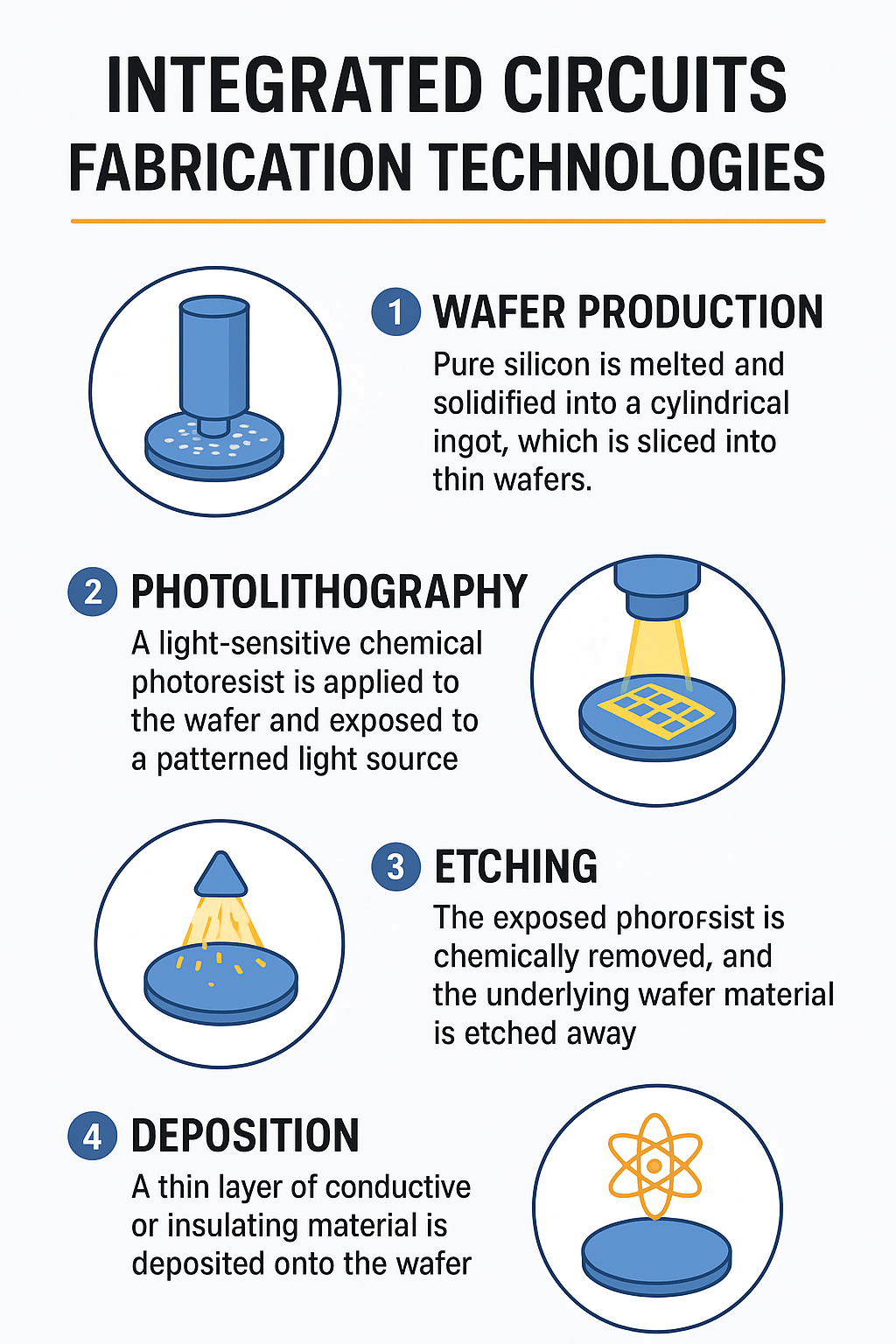
The fabrication of integrated circuits is carried out in semiconductor foundries, often called fabs. Below are the core technologies used in IC manufacturing:
1. Wafer Preparation
The process begins with a pure silicon crystal grown in cylindrical form, known as an ingot. The ingot is sliced into thin wafers, polished to a mirror finish, and cleaned. These wafers serve as the foundation for IC fabrication.
2. Photolithography
Photolithography is one of the most critical steps in IC fabrication. It involves transferring a circuit pattern onto the wafer using ultraviolet (UV) light.
Steps include:
- Applying a photoresist layer on the wafer.
- Exposing the wafer to light through a mask.
- Developing the exposed areas to reveal the desired pattern.
Modern ICs use Extreme Ultraviolet Lithography (EUV) to achieve feature sizes below 7nm.
3. Doping (Ion Implantation)
To create electronic properties, certain regions of the silicon wafer are doped with impurities such as boron, arsenic, or phosphorus. Doping modifies the electrical characteristics, forming p-type and n-type regions required for transistor operation.
4. Etching
Etching removes unwanted material from the wafer surface to define microstructures. Two main methods are:
- Wet Etching: Uses chemical solutions to dissolve materials.
- Dry Etching (Plasma Etching): Uses plasma to remove materials with higher precision.
Dry etching dominates in advanced IC manufacturing due to its ability to produce smaller and more accurate features.
5. Deposition
Thin films of materials are deposited on the wafer to form layers of transistors and interconnections. Common deposition methods include:
- Chemical Vapor Deposition (CVD)
- Physical Vapor Deposition (PVD)
- Atomic Layer Deposition (ALD)
These techniques allow for the creation of conductive, insulating, and semiconducting layers.
6. Chemical Mechanical Planarization (CMP)
To ensure each layer is flat and uniform, wafers undergo polishing through CMP. This step prevents defects in subsequent layers and ensures reliable device performance.
7. Metallization
After the transistor structures are built, metal interconnects are added to link them together. Materials like copper and aluminum are used to form the pathways that carry electrical signals.
8. Packaging and Testing
Once the wafer is complete, it is cut into individual chips. Each chip is packaged for protection and electrical connection, then tested for functionality and performance before being shipped to customers.
Advanced Integrated Circuits Fabrication Technologies
As demand for faster and more efficient electronics grows, advanced IC fabrication techniques have emerged:
- FinFET (Fin Field-Effect Transistor): A 3D transistor structure that improves control over current flow and reduces leakage.
- Gate-All-Around (GAA) Transistors: A next-generation architecture expected to replace FinFETs in sub-3nm technology.
- 3D ICs: Stacking multiple layers of ICs vertically for greater performance density.
- EUV Lithography: Enables features as small as 2nm, driving Moore’s Law forward.
Challenges in Integrated Circuits Fabrication Technologies
Despite rapid progress, IC fabrication faces several challenges:
- Scaling Limits: As transistor size approaches atomic levels, quantum effects create new barriers.
- Cost of Manufacturing: Building and maintaining fabs can cost billions of dollars.
- Heat Management: As density increases, chips generate more heat that must be dissipated.
- Supply Chain Issues: Global semiconductor shortages highlight the vulnerability of fabrication ecosystems.
Future of Integrated Circuits Fabrication Technologies
The future of IC fabrication lies in:
- Sub-2nm Nodes: Driving miniaturization beyond current boundaries.
- Integration with AI and Quantum Computing: Specialized chips for new computing paradigms.
- Green Manufacturing: Reducing environmental impact of energy-intensive fabs.
- Global Expansion of Fabs: Countries are investing heavily to reduce reliance on foreign semiconductor manufacturing.
Conclusion
Integrated Circuits fabrication technologies are the foundation of modern electronics. From wafer preparation to advanced lithography and packaging, each step contributes to the functionality and performance of the final chip.
As industries demand smaller, faster, and more energy-efficient devices, semiconductor manufacturers are pushing the boundaries of physics and engineering. The evolution of fabrication technologies will continue to define the future of computing, communication, and innovation.